

Publisher: Administrator Date:2022-08-26
Wafers are the carriers of chips, and the application of testing equipment runs through the entire process during manufacturing. Wafer testing is key to ensuring stable performance and improving the yield rate. However, issues such as high testing costs and long testing cycles have long constrained the production capacity of wafer manufacturers.
As a leader in the field of semiconductor automated testing, SPEA has keen market insight and technological foresight. It began to focus on the research and development,manufacturing, and continuous improvement of wafer testing equipment many years ago.
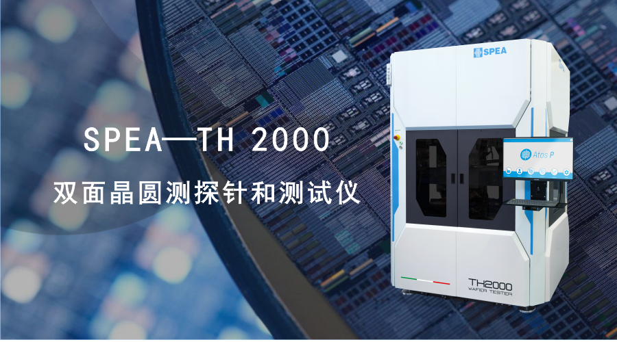
Since its launch, SPEA's TH2000 double-sided wafer tester has successively cooperated with dozens of well-known wafer manufacturers around the world,becoming a good helper for them to reduce costs and increase efficiency.
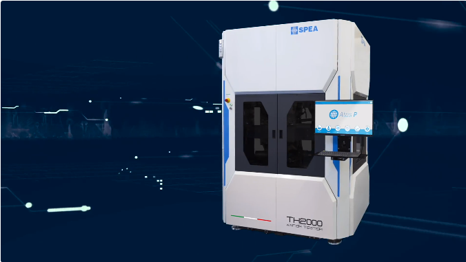
The TH2000 is a revolutionary product that combines double-sided wafer probing capabilities with comprehensive testing resources, integrating practical functions such as electrical testing, HV/HI testing, warpage and surface verification, and optical inspection.
Based on advanced multi-function flying probe card testing technology and a lean testing process, the TH2000 empowers users with more robust comprehensive wafer-level testing capabilities, significantly reducing testing costs. It is suitable for highly challenging tests, including power devices, optoelectronics, through-wafer bare dies, multi-project wafers, complex system-on-chip, and unconventional layouts, with sizes up to 12 inches (300 mm).
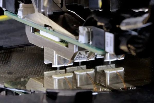
Simultaneous double-sided probing and testing
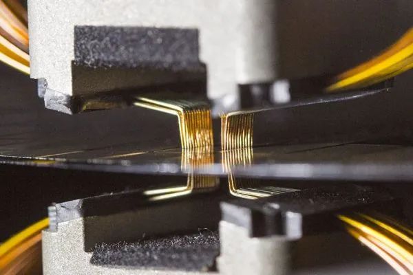
Eight independent axes provide parallel testing functions, thereby shortening the overall process time (indexing + testing time). Each probe can test dedicated areas of the medium in parallel with other probes, while a single wafer can be contacted simultaneously from both the top and bottom.
Planarity and positional compensation
The Z-axis height is analyzed for contour, and each axis automatically compensates to overcome any planarity issues. The precise positioning of the wafer surface through rotational translation is monitored and compensated as needed.
Fast and precise probing
Each XYZ axis utilizes high-speed linear motors with high-resolution linear optical encoders to ensure high throughput and optimal probing accuracy. The system chassis, made of natural granite, offers high rigidity, excellent vibration damping, and thermal stability, preventing any loss of accuracy due to movement speeds and environmental changes.
Gentle contact
Thanks to programmable overload (as low as 1 gram) and controlled motion profiles, the ultra-soft touch technology enables the TH2000 to contact the finest and smallest dies without leaving a trace.
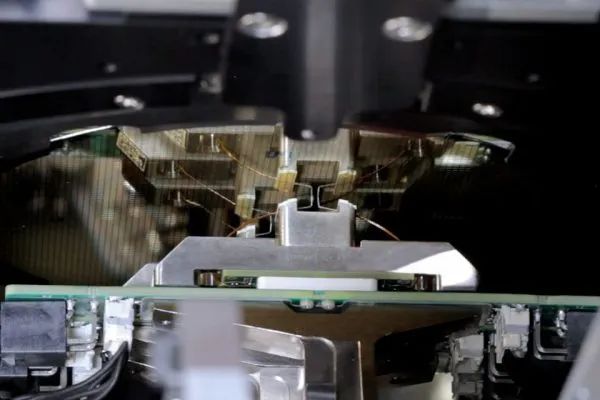
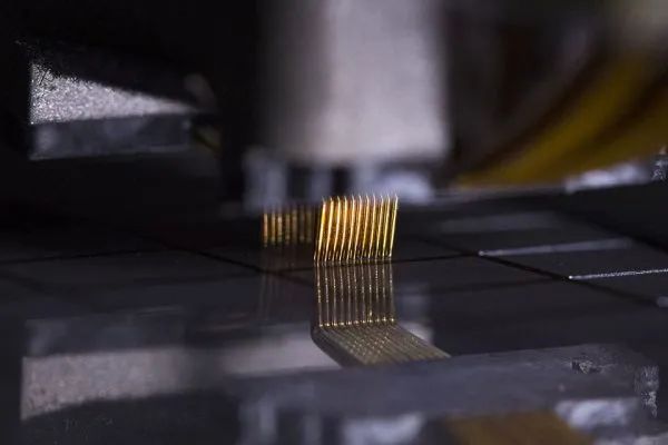
Flying multi-probe card
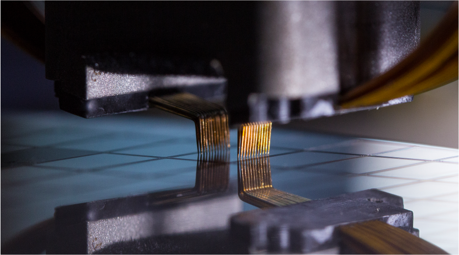
The TH2000 brings the versatility of flying probe technology to semiconductor manufacturers. Each TH2000 axis can be equipped with a single-point or multi-point probe card, featuring different wafer shapes or pitches, including unconventional and high-density geometries. Different probe cards can be installed on different axes, making the TH2000 also suitable for testing multi-project wafers.
Probe cards can be based on different technologies (cantilever, spring probe, MEMS probe, wiring probe), and can be designed according to the density/shape/distribution of each die: testability issues are no longer a limitation of your wafer layout, and can be designed to minimize the cost per die.
Multi-functional flying head
The TH2000 axis can be equipped with single or multiple die probe cards, laser meters, and high-resolution vision units to perform all required tests. Electrical testing includes analog, digital, mixed-signal, high-voltage, and high-current testing.
It can place miniature device under test (DUT) boards with signal conditioning resources directly on the system's flying axes for closer proximity measurements, achieving more accurate test results. It can also probe the same pad on both sides simultaneously, allowing for precise measurements unaffected by adjacent pads.
Mechanical testing includes planarity, height, and warpage tests. Optical inspection can detect scratches, photolithography and pattern defects, particle presence, cracks, and flaws.
Lean testing process
The TH2000 consolidates all required wafer-level testing into a single step, allowing wafer manufacturers to achieve high throughput and cost-effectiveness with fewer testing devices. It can not only accept manual product loading but also operate in a recirculation mode within the test cell and integrates with automatic loaders.
Under the impetus of Moore's Law, semiconductor chip manufacturing technology will continue to rapidly improve, and the value of wafer testing equipment in the semiconductor field will become even more prominent. SPEA has already delivered satisfactory results to major wafer manufacturers, and in the future, SPEA will continue to innovate and explore, providing faster and more efficient solutions for different testing scenarios and requirements.