

Publisher: Administrator Date:2024-03-26
Since its introduction over a decade ago, solder paste jetting has continuously improved the product quality and versatility of electronic manufacturers worldwide. This is particularly true in the high-mix electronics sector, where the high precision and flexibility of software-driven assembly processes are crucial for competitiveness. Now, with faster jetting speeds, a broader range of compatible solders, and tightly integrated solder paste inspection (SPI) functions, jetting technology has matured into a powerful platform that enhances production efficiency and increases first-pass yield.
Significant enhancement in flexibility.
Manufacturers who have replaced steel stencil printing with jetting technology have achieved greater returns in operations, finance, and business benefits. By eliminating the lead times and costs associated with the procurement and management of steel stencils throughout the entire product lifecycle—from cleaning and storage to redesign and replacement—jet printing has reduced production costs, shortened lead times, and enhanced the ability to respond to unexpected changes in production schedules.
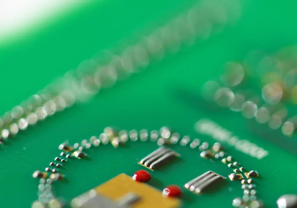
As PCBs become increasingly complex and components more miniaturized, jetting machines capable of a minimum dot size of 210μm can achieve extremely high precision while maintaining the highest level of quality and performance. Under the same workshop skill and resource conditions, jet printing enables suppliers to be more capable, responsive, and attractive when facing the rapidly changing demands of customers.
Dozens of solder pastes, one standard nozzle.
with leading PCB manufacturers, solder paste producers are also becoming increasingly aware of the advantages of the MY700 jetting machine. Today, top manufacturers such as Kester, Koki, Tamamura, AIM, Almit, Alpha, Henkel, and Indium Corporation closely collaborate with Mycronic, not only adapting their best-selling products but also considering the needs for solder pastes with special properties to fit more specific applications. As a result, dozens of the most commonly used solder pastes on the market are compatible with Mycronic's jetting technology, including low-temperature solder pastes and the latest water-soluble flux pastes, as well as an increasing number of other specialized solder pastes.
The versatility of the standard nozzle makes the MY700 very unique. As a result of years of investment in advanced research and development, the nozzle's multi-patented standard design ensures the accuracy and repeatability of each solder joint, ensuring the highest level of speed and robustness while supporting the widest range of solder pastes in the industry with a standard nozzle.
Advanced inspection combined with flexible jetting.
In high-reliability industries, whether it be medical, automotive, or aerospace, perfect solder joints are just part of the challenge. Since each solder joint must also be controlled, measured, tracked, and traced, 3D Solder Paste Inspection (SPI) technology is absolutely essential. PCB assembly production not only requires meeting at least the IPC-A-610 Class 3 standards, but also recording the geometry of each solder joint. These standards of quality and traceability include precise requirements for specific test points at specific production stages, as well as the recording and traceability of information for each product serial number.
The PI series 3D SPI systems from Mycronic are renowned for their high precision and reproducible 3D inspection performance. Their 360° moiré technology, realized through a unique combination of hardware and software capabilities, compensates for any warping of the circuit board, allowing the system to use the actual surface of each pad as a height reference point (z = 0), regardless of the thickness of the solder resist layer. Consequently, the exact volume of solder paste present on each pad can be measured for height with a resolution accurate to 0.1 μm.
Detect steel mesh or stencil printed circuit boards with the same precision.
This technology is highly precise and can detect the solder joints on steel meshes and stencil prints with the same level of accuracy, even for those on components as small as 01005 or smaller. There is a significant difference in the solder joint profiles produced by these two techniques, as stencil printing tends to create smoother solder joints than steel mesh printing when applying equal volumes of solder paste. However, since Mycronic's SPI technology uses the surface of the pad as its height reference, there is no approximation or interpolation when measuring the actual volume of the solder paste. Therefore, the measurement results are equally accurate regardless of the printing method and type of solder paste used.
While the ability to calculate the volume and shape of the solder paste as accurately as possible is clearly crucial, it is equally important in the field of inspection to compare these calculations with expected outcomes. This comparison between actual and expected results is the only reliable method to determine whether each solder joint is indeed compliant. For stencil printed solder joints, this is typically accomplished by calculating the expected volume of the stencil printed solder paste based on programmed data: a combination of the aperture Gerber data and the stencil thickness. However, for dispensing, calculating the expected volume of the dispensed solder paste becomes more complex, depending on the pad dimensions and the packaging application reduction ratio. Therefore, the PI series 3D SPI does not use stencil Gerber data but instead imports the final program from the MY700, making it the only inspection system capable of calculating the true expected volume of MY700 prints, whether used alone or in conjunction with a stencil printer.
Full Material Inspection System
Additionally, the SMT (Surface Mount Technology) process must take into account the unique viscosity and mechanical properties associated with each type of solder paste. The screenshot below illustrates how the shape of the solder paste can vary depending on the type of solder paste used. To maintain flexibility and efficiency, the SPI (Solder Paste Inspection) system must be capable of inspecting all types of dispensed solder paste with the same level of precision and repeatability, despite their differing behaviors.
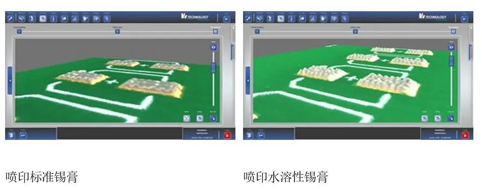
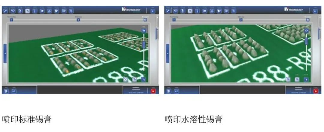
The integration between the MY700 and the PI series SPI 3D allows for the processing of a wide range of material characteristics, accommodating the differences in processing between water-soluble, lead-containing, and lead-free solder pastes. All types of MY700-compatible solder pastes can be inspected by the PI series SPI, even when combined on a single PCB.
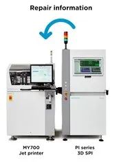
Fully Closed-Loop Inspection
The exchange of information between the PI series 3D SPI and the MY700 enables fully automated control of the printing quality, regardless of the solder paste deposition process - whether it involves stencil printing, dispensing, or a combination of both. Whenever the PI series detects a lack of solder paste, the MY700 can automatically compensate. The SPI only uses the unique ID code of the PCB to inform the dispensing machine which board needs repair and sends information on the location and volume that need compensation. The result is a significant reduction in repair costs, increased first-pass yield, and improved production efficiency. Depending on environmental and production constraints, two configurations can be implemented to target a zero-defect printing process:
High-Mix Production: Repair information is sent back to the dispensing machine.

Mass Production: The dispensing machine can handle solder paste attachments and perform repairs as needed. An additional SPI can be added after dispensing to simultaneously inspect both stencil and dispensed solder.
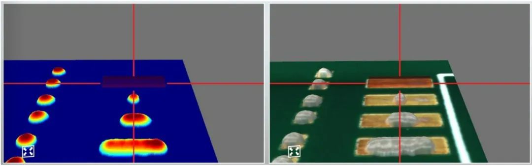
The PI series 3D SPI detects solder paste defects.
The solder paste defects have been corrected by the MY700 dispensing machine.
Towards a Future of Zero Defects.
Regardless of the printing method, type of solder paste, or production environment, these extensive features make dispensing a natural choice for any high-quality, high-flexibility manufacturing environment. Most PCB defects tend to occur at the solder paste printing stage. The MY700, fully driven by software and supported by advanced inspection data, continuously addresses the most challenging quality gaps.